Emerging semiconductor manufacturing technology
MUNICH, August 2, 2016 – ERS electronic GmbH, the innovation leader in the market of thermal test solutions for semiconductor production, sees excellent growth opportunities in the emerging eWLB / FOWLP (Fan Out Wafer Level Packaging) advanced packaging technology. ERS expects this market to grow at a pace of more than 30 per cent annually – and ERS is extremely well positioned to benefit from this situation.
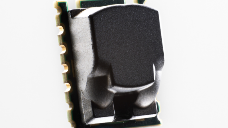
eWLB (Embedded Wafer-Level Ball Grid Array) is a very economical packaging technology for the advanced semiconductor solutions required for innovative application areas such as Internet of Things, sensors, automation and mobility. It enables semiconductor manufacturers to create chips with smaller footprint, thinner package and better electrical properties than possible with conventional flip-chip BGA packaging. Therefore it is a crucial technology to create space-saving yet powerful solutions. Since this technology is already proven in mass production at renowned semiconductor manufacturers and offers substantial technological and cost benefits, it can be expected that it will reach a very high popularity throughout the entire semiconductor industry.
Due to its world-leading thermal expertise, ERS has been involved in the development of this technology from its inception. For more than six years, ERS“ equipment is deployed in the most demanding mass-production environments at leading semiconductor manufacturers and OSATS worldwide. For this reason, ERS has a unique position in the emergent dynamic market for eWLB manufacturing equipment and will fully benefit from the rising demand for such equipment. With its sound experience in thermal treatment as well as in eWLB manufacturing processes, ERS can support manufacturers to get their processes stable and economic and can adapt its equipment quickly to new requirements.
On the basis of this unique set of capabilities and expertise, ERS has won two major customers in this global market within only six months. Through its eWLB Competence Center, located at the ERS headquarters near Munich, ERS is actively involved into further developing the technology. This enables the company to quickly react on changing market and technology conditions. Even more important, through this Competence Center ERS is an active eWLB technology player and has immediate access to all new developments from their beginning.
ERS electronic GmbH, based in Germering near Munich, has been producing innovative thermal test solutions for the semiconductor industry for 45 years. The company has gained an outstanding reputation in the sector, notably with its fast and accurate thermal chuck systems for test temperatures ranging from -65°C to +500°C for analytical, parameter-related and manufacturing tests. Today, thermal chuck systems developed by ERS in its product families AC3, AirCool©, AirCool© plus and PowerSense© are an integral component in all larger-sized wafer probers right across the chip industry.
Firmenkontakt
ERS electronic GmbH
Klemens Reitinger
Stettinerstraße 3+5
82110 Germering
+49-89-8941320
kreitinger@ers-gmbh.de
http://www.ers-gmbh.com
Pressekontakt
Brand+Image
Timothy Göbel
Von-Eichendorff-Str. 41
86911 Dießen a.A.
08807 9475642
ERS@brandandimage.de
http://www.brandandimage.de

